Catching Waveguides and Controlling Light
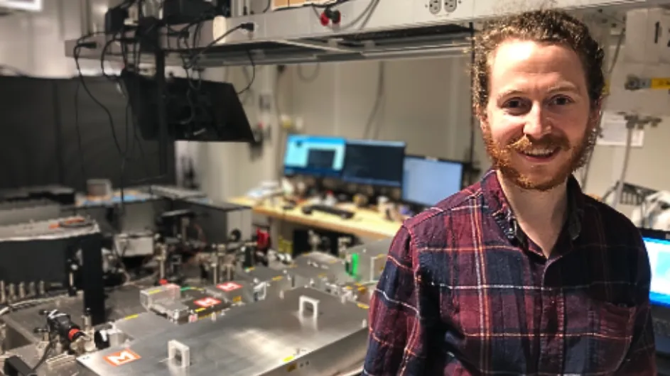
Columbia postdoc Samuel Moore explains his recent research on waveguides in 2D materials, published last month in Nature Photonics.
If you shine light onto a material, its electrons gain some energy and become excited. The excitement can’t last, however, and when the electrons inevitably return to their baseline energy, they spontaneously emit discrete packets of light called photons. With a little guidance, in the form of what’s known as a waveguide, researchers can gain control over the emitted photons.
Dmitri Basov’s lab at Columbia is pushing that control to the atomic limit—and beyond—by taking advantage of the unique quantum properties of atom-thin two-dimensional materials. In a paper published last month in Nature Photonics, the Basov lab and collaborators directly capture the waveguiding properties of 2D materials with a new nano-optical imaging technique. The research was led by Samuel Moore, who graduated this spring with his PhD in physics and is staying on for one more year at Columbia as a postdoctoral fellow.
In this Q&A, Moore explains the importance of waveguides in quantum materials and shares some highlights from his time at Columbia.
What were you exploring in the Nature Photonics paper?
A lot of the work we do in the Basov lab involves waveguides. Waveguides are physical structures in materials that channel light in a certain direction. This confines the photons to areas that are smaller than the usual wavelength of light and enhances the strength of the electric field inside the material.
We were studying how waveguides can control the spontaneous emission of light from a material, a key hallmark of what’s known as quantum electrodynamics (QED), a fully quantum description of light-matter interaction.
What materials were you working with?
We were working with only 2D materials: we sandwiched a single layer of MoTe2, which spontaneously emits light in response to a laser, between WSe2, another 2D material that naturally hosts waveguided light.
What was your main result?
We directly observed what’s known as the Purcell effect, which is the speeding up of the spontaneous emission rate of photons through a waveguide. Because waveguided light is confined inside the material, you can’t see things with a normal microscope and have to rely on counting photons over time to see if the spontaneous emission rate is changing, but that doesn’t always confirm the Purcell effect.
To observe the effect, we scanned the surface of our sample with a sharp tip, which acts as an antenna for the confined light. With our new nano-optical imaging technique, we were able to see the confined photons move through the waveguides, confirming that these structures can control spontaneous emission rates, as QED theory predicts.
Why is that exciting?
Creating waveguides currently involves time-expensive lithography to pattern crystals with the structure that you want. But we don’t need to do any of that! Thin flakes of WSe2 can be peeled from a crystal with just Scotch tape. There’s a convenience factor to working with these 2D materials.
Eventually, they may become integrated into photonic chips, reducing the footprint required for the light source that can produce a very bright light.
What’s next for this line of research?
Different materials will have different waveguiding properties. Others might confine the light even better, which would mean an even higher Purcell enhancement.

But it takes the right materials. When I started this project, I was stacking different materials a bit randomly; everything was dark, nothing was working, until I found the right combination. Just seeing the pattern show up was a standout moment.
Currently, we’re working on a “self-waveguide” compound– one that emits light and acts as a waveguide all in one material, further simplifying the device geometry.
How did you end up at Columbia?
I did my undergraduate degree at MIT and was initially interested in theoretical high-energy and astrophysics. But then I started doing some optical experiments. I liked tabletop experiments and getting to look at real materials.
After I graduated, I spent a year working with Andrea Cavalleri at the Max Planck Institute for the Structure and Dynamics of Matter in Hamburg. It was a lot of optics work, shining lasers on different materials, and I really got my feet wet with quantum materials. At Columbia, I became interested in going further into quantum optics and QED, while building samples myself and doing the different measurements.
What other materials have you worked with here?
My work generally examines light-matter interactions at small length scales. Previously, for instance, I studied nanoscale variations of vibrational modes in a moire superlattice formed by two twisted layers of a material called hexagonal boron nitride.
And what’s next for you?
I’m starting to look for academic jobs. There are a lot of different directions to go, but I hope to continue working in the field of quantum optics and materials.
What keeps you busy outside the lab?
I’m a musician, mostly playing piano at home these days, and I enjoy going to jazz concerts around the city with my wife. There’s great music here—plus, great food and great coffee.