A Toolbox for Creating Quantum Effects
The ability to program desired properties into materials will be key for making quantum technologies work in the real world. At the Programmable Quantum Materials Energy Frontiers Research Center, researchers have come together to create quantum effects on demand

Observations are the foundation for much of physics. Progress happens by taking measurements and trying to understand what just happened. Some quantum researchers, however, have even higher aspirations.
“We don’t just want to observe quantum effects,” said Columbia physicist Dmitri Basov. “We want to create them.”
The quantum world exists at a scale beyond classical physics, at the level of molecules, atoms, and subatomic particles. There, things don’t behave exactly how we are used to. Particles like electrons and photons of light move in wave-like patterns that can only be explained by statistical probabilities. There’s still much to learn, but at the Columbia-based Programmable Quantum Materials Energy Frontiers Research Center, researchers have been working to add an element of control to quantum physics, which could help bring about another technological revolution.
“Human society has evolved, from the Stone Age to now, as we discovered and learned how to use new materials, ’ said co-investigator Xiaodong Xu, a professor at the University of Washington. Creating and controlling new quantum materials will be key to building the next evolution of devices, like quantum computers, quantum sensors, and new kinds of lasers.
Led by Basov at Columbia, and with collaborators at Washington and Brookhaven National Laboratory, the Center’s unique group of researchers have been at work for nearly four years establishing new materials, physics, and tools to manipulate the quantum world.
Meet the Quantum Makers
The search for new physical phenomena often begins with new materials, a domain that synthetic chemists specialize in. “We’re the makers—not the measurers,” said Xavier Roy, a Columbia chemist and member of the Center. Roy’s lab makes van der Waals crystals made up of stacked sheets of materials that are weakly held together. Once synthesized, the millimeter-sized crystals can be peeled into component layers that are just a single atom thick. These two-dimensional, van der Waals materials have been the main focus of the Center’s research.
As you move from three dimensions to two, weird things start to happen, said Roy. Cadmium selenide is a classic example. In three dimensions, it’s a dark reddish-black crystal; shrink it down, and the color changes. Other characteristics can also change in 2D, such as magnetism and electrical conductivity. This is exemplified by chromium sulfide bromide, a van der Waals crystal synthesized in Roy’s lab a few years ago. After spending some time exploring the properties of the bulk crystals, the lab peeled off some layers and gave them to collaborators at the Center, including Xu at Washington and Xiaoyang Zhu at Columbia.
As both labs dug into the physical properties of the 2D sample, they discovered three unique features: chromium sulfide bromide is magnetic, it can conduct an electrical current, and it emits light. “If a material has multiple functions, those may couple and generate new phenomena," said Zhu. “That’s exactly the case here.
Shining a light on certain semiconducting materials creates particles called excitons that give a crystal its specific color, said Zhu. But chromium sulfide bromide is different. Applying a magnetic field to it switches the direction that its electrons spin, which changes the emitted color. “This is the first example in materials science where you can change the color with a magnet,” said Zhu. Electron spin is a quantum state that can be used to record information; having a color-based read-out of that state could help researchers develop novel chips for devices, he said.
Making materials can be an intentional process, with chemists building on existing knowledge to predict how a certain combination of elements might crystallize and behave. Or it can be serendipitous. Many of Roy’s lab members combine atomic elements, heat them up, and see what happens. “There’s a lot of chemical intuition,” said Roy. “That’s what a lot of chemistry is: just figuring out how to make new materials.”
Crystals, though, aren’t always as pretty as they appear in papers. An atom in the crystal lattice may be missing, or in the wrong position. Sometimes imperfections bring about a desired property; other times, they’ll interfere. Other labs, including Center collaborator James Hone’s, have been developing techniques to make 2D materials with more reliable compositions and structures.
Dialing In New Properties to Materials
Two-dimensional materials are relatively easy to manipulate. Electrodes to apply electrical currents can have constant contact across the surface of each layer, and layers can be stacked in different arrangements. “Because they are atomically flat, the layers can talk to each other,” said Roy. That feature brings with it even more strange behaviors that the Center is now figuring out how to control.
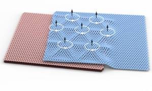
When stacked layers of van der Waals materials are twisted, they form a Moiré pattern. Changing the angle of the twist, along with temperature and electrical and magnetic fields applied to the material, can change its properties. It’s pretty sci-fi, said Basov. “You can dial in the properties you want, almost like a rotary phone, but at a nanoscale.”
The Center’s experiments with twisted van der Waals materials have revealed new insights into quantum phenomena such as superconductivity, the resistance-free flow of electricity, and quantum criticality, the point where one quantum phase transitions to another. Twisting has also been used to trap individual particles and produce an entirely new flavor of magnetism: orbital magnetism, based on the coordinated rotation of electron motion in the sample. The resulting magnetism can be adjusted by adding or subtracting electrons in a process called doping, and by applying different magnetic fields. “These are all different knobs that give us direct and predictable control,” said Matt Yankowitz, an assistant professor at the University of Washington and former Columbia postdoc.
The Center is now starting to harness quantum effects by tweaking 2D materials. In James Schuck’s lab at Columbia, researchers are exploring whether 2D materials could be useful as quantum light sources that will reliably emit photons in a desired color, number, and frequency—a level of control necessary for quantum hardware.
Certain crystals can produce individual photons, but their properties are fixed: the color they give off is all you get. Two-dimensional materials potentially offer more variety. In 2020, Schuck and his colleagues showed that bilayers of tungsten diselenide, a 2D material manufactured in Hone’s lab, could be coaxed into producing single photons with the introduction of strain. They are now exploring how photons produced by such manipulations can be further tweaked.
"You can dial in the properties you want, almost like a rotary phone but at a nano-scale"
Bringing New Materials into Focus
As new materials are developed and manipulated, researchers also need ways to observe and characterize what’s happening. Probing materials with the light from a microscope is a common way to do this, but their focus is usually limited to a spot roughly equivalent to its wavelength, measured in micrometers rather than the nanometers needed to observe quantum properties. “There’s been this mismatch between the length scales,” said Schuck.
At Washington, physicist David Cobden has been improving a technique called angle-resolved photoemission spectroscopy (ARPES), which he and collaborators have used to image electronic structures within 2D materials for the first time—previously, the only way to learn what electrons were doing was with complicated models. “We can directly measure the electronic spectrum in detail and see how it changes in real time,” said Cobden
The ARPES device is used at the Spectromicroscopy Beamline at the ELETTRA synchrotron in Italy. Back at tabletops and research benches on the East Coast, there have been advances with scattering near field optical microscopes, or SNOMs. Pre-Center (and appointment at Columbia) Basov’s group built the first cryogenic version of the microscope, which combines nanoscale tips that can detect changes when that sample is hit with a particular wavelength of light. The microscope measures the resulting change of “color,” allowing researchers to visualize phase transitions and hybrid particles made of light and matter called polaritons.
It took years to develop their first microscope, but the Basov Lab recently built two successors in just a few months. While the first-generation microscope can image samples with mid-infrared range light, the subsequent devices can now capture long-infrared and visible wavelengths of light as well. By adding additional light sources, they’ve added a timestamp to their experiments: one beam of light arrives first and alters the sample, while a second beam arriving later captures the change.
A hybrid instrument that combines existing instruments developed at Columbia in one universal platform is also in the works. Individual instruments are fine, but, said Schuck, “it’s been difficult to take a sample from one instrument and stick it in another.” The ability to take multiple measurements from the same sample will let researchers link different pieces of information and gain deeper insight into how these materials work and behave, he said. “You just need the right set of expertise to implement.”
Images are also getting sharper as alternatives to current probes in nano-optical instruments are developed. Schuck has been exploring lanthanide materials, synthesized in Roy’s lab, that change with their environment. Schuck and colleagues recently demonstrated a phenomenon called photon avalanching in a ~25 nm lanthanide nanoparticle, which they are using to turn conventional microscopes into super high-resolution imaging systems.
All of these instruments use light to probe the properties of a sample but in the future, light may also be used to control materials, too. In some of the Center’s most recent work, they’ve been starting to build new electronic and photonics states. "Laser pulses allowed us to create a new electronic state in this prototypical semiconductor, if only for a few picoseconds," said Basov. "This discovery puts us on track toward optically programmable quantum phases in new materials. "
An On-Demand, Ready to Use Quantum Toolbox
The Center’s ultimate goal is to develop materials that can make quantum computers and simulators possible, advance quantum information, and guide others in search of quantum applications for everyday life. “If we can do that, that’s a major contribution,” said Zhu.
“We’re discovering new quantum material platforms with programmable properties,” said Yankowitz, along with new instruments to study them. “Once you have all those tools in your toolbox, you’re in a position to start putting them together.”
Read More:
Collaboration has been a key ingredient, with each faculty member from each university bringing unique expertise in theoretical physics, experimental design, and engineering disciplines. The group, said Basov, plays as an orchestra, with each participant adding their own sound for a magnificent effect: in just three and a half years, the Center’s 19 principal investigators (which includes several junior faculty) and 21 postdocs and graduate students have published more than 80 papers with over 5,500 citations. Next time, said Basov, they’ll set the bar even higher as they start putting their on-demand quantum toolbox to use.
The Programmable Quantum Materials Energy Frontiers Research Center is supported by the United States Department of Energy under Award DE-SC0019443. The Center thanks their External Advisor Board, Drs. Eve Andrei, Nuh Gedik, Andrew Kent, Jeremy Levy, and Eugene Mele, for their time and helpful advice.
For more research highlights and information about the Center, visit the Columbia Programmable Quantum Materials EFRC website or contact Dr. Dmitri Basov, Pro-QM Director.


